
Terms & Acronyms
- PCB – Printed Circuit Board.
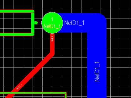
- Tracks – Form the connections between component.
- Pads – Used to make connections between your component and the track with solder.
- Layers - Everything is drawn on a layer, layers can have different physical properties. Example layers are: Top layer, bottom layer, Top overlay, bottom overlay, Mechanical 1, Keep Out.
- Plated Through Holes (PTH) – Drilled holes that are plated with conductive material (usually copper).
- Footprints – A collection of pads and outlines which describe an individual component’s physical layout on a PCB.
- Design Rules – Rules specified by the designer to ensure PCB integrity (more on this later).
- Vias – Used to make connections between differentlayers of the PCB.
- Silkscreen – A protective layer over the top of theboard, makes soldering easier.
Some more doubts to clear......
FAQ
1. Should I use metric or imperial?
2. What size drill-holes should I be using?
3. What size should my tracks be? What sort of clearance should I have
between tracks?
4. The tutors tell me Auto-route is the Devil, is this true?
5. Help! I can’t find a footprint for my component!
1. Should I use metric or imperial?
• Remember: Metric measurements are in (milli)meters, imperial
measurements are in thou (thousandths of an inch).
• For Team Project PCB's we have decided on the following important rules.
• 1000mil/thou = 1 inch ≠ 1000mm.
• Drill Holes – USE METRIC!
2. What size drill-holes should I be using?
• If a panel to be manufactured has more than 15 different hole sizes, then
the COST increases and possibly even the LEAD TIME. So try to use as few
as possible (within reason).
Suggested Hole Sizes
Part
|
Suggested
Hole size
|
| Vias | 0.6mm |
| IC Legs, TO-92 Transistors, 1N4148 Diodes | 0.9mm |
| Resistors/Capacitors/ and many other components | 0.8mm |
| Diode Legs (1A, eg 1N4004), IDC connectors, TO-220 transistors | 1.0mm |
| Diode Legs (3A, eg 1N5404), many connectors | 1.25mm |
4. What size should my tracks be? What sort of clearance
should I have between tracks?
• A track should not be narrower than the minimum manufacturing limit.
However, it is recommended that for simple designs you should stick to
12thou (0.3mm) as a minimum.
• Thicker tracks are needed if you want to carry significant current. Thin tracks
will get hot, and cause voltage drops if significant current flows.
• For your projects, there’s no harm in using larger tracks.
5. The tutors tell me Autoroute is the devil!
• Using Autoroute is a design decision of your own to make.
• Using Autoroute is a lazy option (you should be spending more time learning
how to create PCBs, not less). “Would you trust Microsoft Word to
automatically format
6. Help! I can’t find a footprint for my component!
"MAKE YOUR OWN"
(More on this soon)
General PCB Design Tips
PCB Design Tip 1: LABEL YOUR PCB
•Include your TEAM NUMBER & COURSE CODE
Put it on Top Overlay

PCB Design Tip 2: Be careful with your power nets
•Place decoupling caps near microcontrollers and other IC's, to
help reduce noise on your power-supply line. How much
capacitance? If the datasheet don’t specify an amount, start
with 10-100nF, then measure your supply-line using a CRO.

PCB Design Tip 3: Orientate polarised components sensibly

PCB Design Tip 4: Where did that component go?
Make use of the PCB filter

PCB Design Tip 5: Make sure you draw a PCB border on Mechanical Layer 1
OTHERWISE YOUR PCB MAY BE REJECTED!
PCB Design Tip 6: If you make mistakes on your board, it is possible to correct them with PCB hacks.
• Cut tracks with a sharp knife.
• Bridge tracks/pads with fly-wire.
• File/cut your board down to size. Wear a mask.
• Drill new mounting holes (if you forgot them!).
PCB Design Tip 7: Use oval shaped solder pads instead of circular
pads.

PCB Design Tip 8: Use long solder pads for surface mount
devices.

PCB Design Tip 9: Learn how to use the Bill of Materials tool!
You can keep track component details such as:
• Part Manufacturer
• Supplier (and cost)
• Supplier order number
• Datasheet URL
• etc
PCB Design Tip 10: Spend lots of time setting up your PCB rules!
Eg
• Set your Power Nets to have a minimum track
width of 18mil.
• Set your ground plane to have a larger
clearance constraint than usual.
PCB Design Tip 11: Make sure you check the PCB manufacturing
rules!
Or your board will not be accepted!
PCB Design Tips
• Use a sensible number of drill-hole sizes. (Consolidate with other teams).
• Don’t forget mounting holes!
• If your PCB has a background layer, delete it!
• Take your time (and allocate a lot of it). You can’t do a PCB design the night before a batch is due.
NUMBER ONE PCB DESIGN TIP
"PRINT YOUR PCB TO SCALE AND PLACE COMPONENTS ON TOP OF YOUR PRINTED PCB".
7 comments:
Electronics manufacturing service I think this is an informative post and it is very useful and knowledgeable. therefore, I would like to thank you for the efforts you have made in writing this article.
Altium Designer Crack I am very impressed with your post because this post is very beneficial for me and provide a new knowledge to me
I guess I am the only one who comes here to share my very own experience guess what? I am using my laptop for almost the post 2 years.
Altium Designer Crack
Renee iPhone Recovery Crack
MorphVox Pro Crack
Very good article! We will be linking to this particularly great post on our website. Keep up the good writing.
Renee iPhone Recovery Crack
CorelCAD Crack
Blackmagic Design DaVinci Resolve Studio Crack
Such a Nice post. Thanks for Awesome tips Keep it up
renee-iphone-recovery-crack
Your style is so unique compared to other people I have read stuff from. Many thanks forposting when you have the opportunity, Guess I will just bookmark this site Altium Designer
I guess I am the only one who came here to share my very own experience. Guess what!? I am using my laptop for almost the past 2 years, but I had no idea of solving some basic issues. I do not know how to Download Cracked Pro Softwares But thankfully, I recently visited a website named vstfull.com
Renee iPhone Recovery
Snapchat
Arturia Analog Lab
Post a Comment